 en
 kor
 de
 jp
 pl
 pt
 it
 fra
 vie
 may
 fil
 th
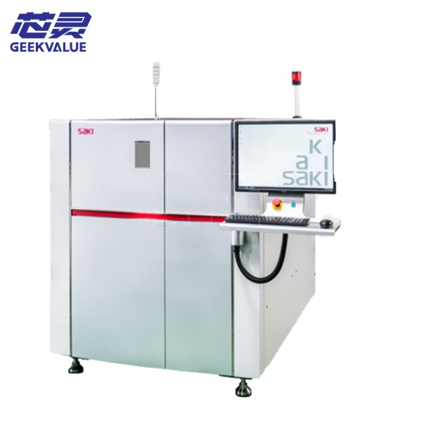
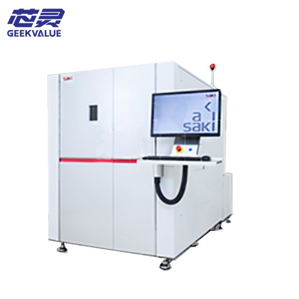
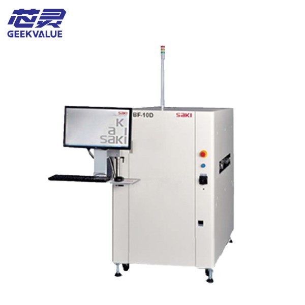
BGA solder joints, concealed connections and internal assembly structures cannot be fully evaluated from the outside of a component. The BF-3AXiM110 uses X-ray imaging to reveal internal features, giving inspectors another way to investigate defects that surface-level optical inspection may not expose.
Published third-party listings for this model report a maximum PCB size of 510 × 460 mm and sample-stage travel of 500 × 500 × 200 mm along the X, Y and Z axes. The same listings describe 2D imaging and 3D CT inspection, with an optional rotation configuration. These figures should be checked against the actual machine documentation before being used as purchase specifications.
For CT inspection, sample positioning and rotation capability affect the views available for examining internal structures. Image resolution and scan time also depend on the selected imaging mode and inspection conditions. A specification comparison should therefore distinguish 2D imaging performance from full CT scanning rather than treating them as the same measurement.
SAKI BF-3AXiM110 3D Specifications
| Item | Specification |
|---|---|
| Brand | SAKI |
| Model | BF-3AXiM110 |
| Inspection Method | X-ray imaging; 3D CT capability reported |
| Maximum PCB Size | 510 × 460 mm, reported; confirm |
| Sample-Stage Travel | 500 × 500 × 200 mm, reported; confirm |
| Rotation / Tilt | Confirm installed configuration |
| X-Ray Source | Confirm machine nameplate |
| Image Resolution | Confirm mode-specific specification |
| Power and Safety Requirements | Confirm original equipment documentation |