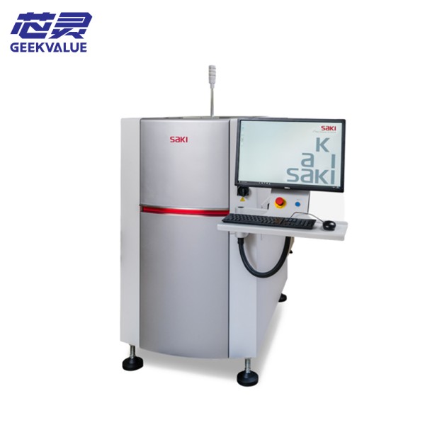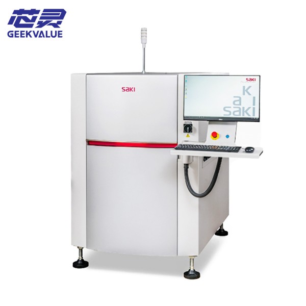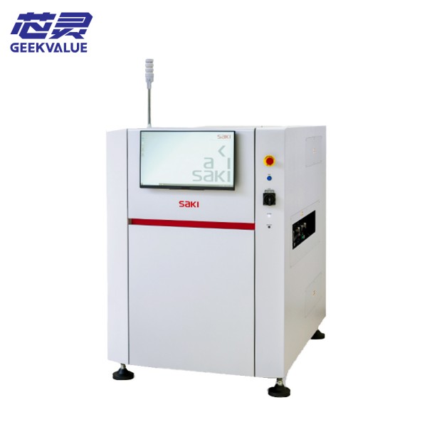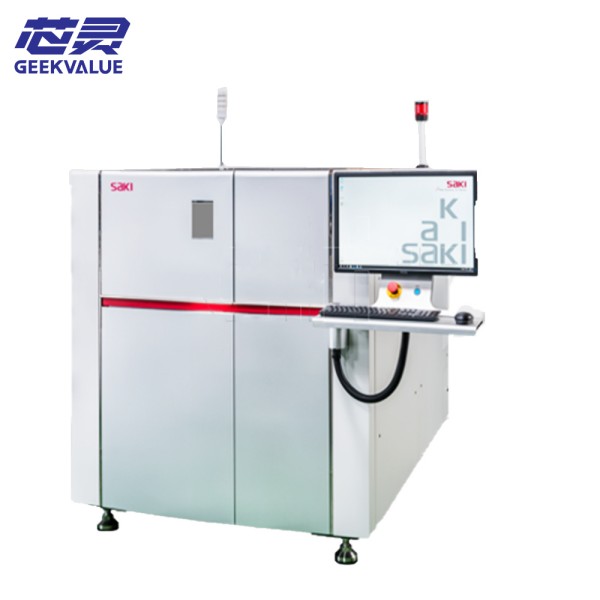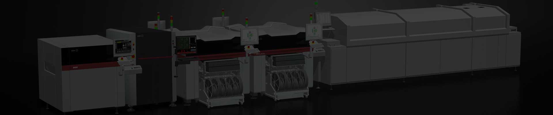
SAKI X-RAY BF-3AXiM200 Full Technical Detail
1. Product Overview and Core Advantages
Product Positioning
SAKI BF-3AXiM200 is a high-end 3D X-ray automatic inspection system developed by SAKI of Japan, mainly for:
High-density packaging (such as FC-BGA, SiP)
Automotive electronics (ADAS module, power module)
Military industry and aerospace (high reliability PCB)
Five core advantages
Three-axis linkage CT scanning: X/Y/Z axis synchronous movement to achieve true 3D imaging
Nano focus X-ray tube: 0.3μm resolution (industry leading)
AI defect analysis: Deep learning algorithm automatically classifies 30+ types of welding defects
Dual energy spectrum imaging: Can distinguish different solder compositions such as Sn/Pb/Ag
Intelligent safety protection: Radiation leakage <1μSv/h (far lower than the national standard)
2. Technical specifications and system composition
Hardware configuration
Subsystem Technical parameters Features
X-ray source 160kV/65W closed tube Tungsten target, life ≥ 50,000 hours
Detector 2048×2048 pixel flat panel 100fps dynamic acquisition
Mechanical system Linear motor drive Repeat positioning accuracy ±2μm
Protection system 0.5mm lead equivalent Door interlock + emergency stop double insurance
Key performance indicators
Parameters Indicators
Maximum inspection board size 610×508mm
Minimum detectable defect 0.5μm (copper wire open circuit)
3D reconstruction accuracy ±5μm@50mm FOV
Typical inspection speed 15 seconds/slice (200μm layer thickness)
3. Detection capability and software functions
Detection items
Soldering defects:
BGA/CSP: voids, cold soldering, bridging
Through-hole soldering: insufficient tin filling, wicking effect
Assembly defects:
Component displacement, missing, polarity error
VisionX3D software functions
Intelligent detection mode:
Automatic slice planning (supports tilt scanning)
3D virtual sectioning (observation at any angle)
Data analysis:
Void rate statistics (compliant with IPC-7095 standard)
Automatically generate ORT report (including 3D model)
4. Installation requirements and operating specifications
Site preparation
Project requirements
Ground load bearing ≥1500kg/m²
Ambient temperature 20±3℃ (constant temperature)
Humidity range 30-60% RH
Power supply specifications 220V±5%/50Hz (independent grounding)
Safety operation points
Power-on sequence:
Start the water cooler first → then start the X-ray system → finally start the software
Sample placement:
Use ceramic carrier (avoid metal interference imaging)
The board edge is ≥50mm from the bulkhead
5. Common fault diagnosis and treatment
Hardware fault
Code Phenomenon Solution
XE101 X-ray tube overheating Check the flow of the water cooling system (need ≥2L/min)
ME205 Z-axis servo abnormality Restart the driver → Check the cleanliness of the grating scale
DE308 No signal from the detector Re-plug the Camera Link interface
Software fault
Code Possible cause Solution
3DERR07 Reconstruction algorithm failed Reduce the slice thickness (recommended ≥100μm)
AICONF02 AI model loading timeout Update CUDA driver to version 11.4+
DBFULL11 Database is full Clean up historical data or expand storage
Typical imaging problem handling
Blurred image:
Check the X-ray tube focus mode (point/line mode switch)
Clean the detector protection window
Artifact interference:
Perform dark field/bright field correction
Adjust KV/μA parameter combination
6. Maintenance guide
Periodic maintenance
Period Maintenance content Standard method
Daily Dust removal in the cabin Use anti-static vacuum cleaner
Weekly Lubricate moving parts Apply KLUBER grease
Monthly Radiation safety inspection Use 6150AD dosimeter
Quarterly X-ray tube calibration Use SAKI standard calibration parts
Consumable replacement
Parts Replacement cycle Notes
X-ray tube ≥30,000 hours Need to be replaced by the original manufacturer
Detector protective film 12 months Conductive film must be used
Cooling water 6 months Deionized water is required
7. Typical application cases
Case 1: Server CPU socket detection
Challenges:
LGA3647 socket hidden solder joint detection
Requirement of void rate <15% (according to IPC-7095C)
Solution:
Use 60° tilt scanning mode
3D measurement of each solder ball volume
Case 2: Electric vehicle IGBT module
Special requirements:
Detect Al wire bonding status
Distinguish SnAgCu from PbSn solder
Implementation method:
Enable dual energy spectrum scanning (80kV/130kV switching)
Customized AI classification model
Technical summary
BF-3AXiM200 redefines industry standards through three major technological breakthroughs:
Imaging innovation: Nano focus + photon counting detector to achieve submicron level detection
Intelligent analysis: 3D defect automatic classification system based on deep learning
Safety design: Multiple protections ensure zero radiation risk for operators