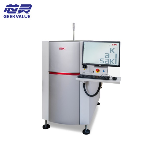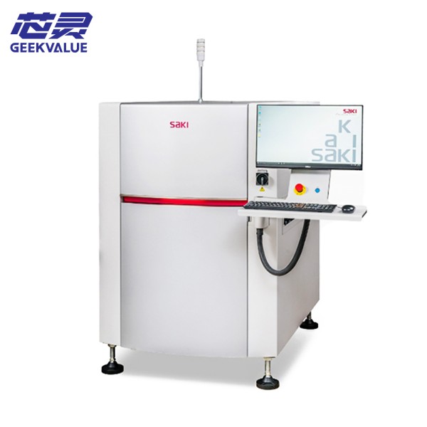
SAKI 3Si-LS3EX is the latest high-end 3D solder paste inspection system (SPI) launched by SAKI of Japan. It adopts multi-spectral confocal imaging technology and is designed to meet the ultra-precision solder paste inspection requirements such as 01005 components and 0.3mm pitch BGA. Compared with the previous generation 3Si-L2, LS3EX has significantly improved the inspection speed, accuracy and intelligence.
Typical application scenarios
Miniaturized electronics: smart watch motherboard, TWS headset circuit board
High reliability field: automotive ADAS module, medical implant device PCB
Advanced packaging: Fan-out packaging, 2.5D/3D IC substrate
2. Technical specifications and hardware configuration
Core hardware parameters
Subsystem Technical specifications Technical highlights
Optical system 7-wavelength confocal imaging (405-940nm) Eliminate metal reflection interference
Z-axis measurement White light interferometer assisted 0.05μm resolution
Motion platform Magnetic suspension drive Acceleration 2G, repeatability ±1μm
Detection range 510×460mm standard version Optional 610×510mm large size
Key performance indicators
Parameters Indicators Test conditions
Height accuracy ±0.5μm 50μm standard step
Volume accuracy ±2% IPC-7527 standard
Minimum detection size 30×30μm 01005 component pad
Maximum scanning speed 1.8m/s Simple graphics mode
Detection cycle <8 seconds/board 300×200mm board
3. Core functions and technological innovation
Revolutionary detection technology
SmartFocus 3.0 technology
Dyamic focus compensation to solve the measurement error caused by PCB warpage
Adaptable to 0.1-1.2mm board thickness change
AI solder paste prediction engine
Predict the shape after reflow soldering (simulate thermal deformation process)
Identify potential bridging/false soldering risks in advance
Multi-process compatible mode
Process type Detection mode
Ordinary SMT Fast scanning mode
Precision packaging High resolution mode (5μm step)
Thick copper PCB Infrared compensation mode
Intelligent software function
Real-time 3D modeling:
Solder paste 3D model example
(Figure: Solder paste volume distribution heat map)
Closed-loop feedback system architecture:
Chart
Code
4. Operating specifications and safety precautions
Standard operating procedures
Preheating before powering on
The laser system needs to be preheated for 15 minutes (extended to 20 minutes when the ambient temperature is <25℃)
Daily calibration
Use the NIST traceable calibration board to execute:
python
def daily_calibration():
if not calibrate_height(standard=50μm):
alert("Z-axis calibration abnormal")
run_flatness_check()
Detection parameter settings
Solder paste type Recommended parameters
SAC305 Wavelength combination: blue + infrared
SnPb Wavelength combination: green + red
Conductive adhesive Special mode M7
Key safety specifications
Laser safety:
It is forbidden to open the protective cover when the equipment is running (in accordance with IEC 60825-1 Class 1M standard)
Special laser protective glasses must be worn during maintenance
Electrical safety:
Check the ground resistance every week (need to be <3Ω)
After a sudden power failure, it is necessary to restart after an interval of 5 minutes
5. Common fault diagnosis and solutions
Hardware faults
Error code Fault phenomenon Processing steps Tool requirements
E701 Laser power attenuation 1. Clean the fiber connector
2. Perform power calibration Optical power meter
E808 Platform vibration exceeds the standard 1. Check the air floating foot pressure
2. Isolate the surrounding vibration source Vibration analyzer
Software failure
Error message Root cause Solution
"AI model loading failed" Insufficient GPU video memory 1. Upgrade the driver
2. Simplify the detection area
"Data storage conflict" Database index is damaged Execute DB_REBUILD command
Typical process problem handling
Solder paste edge jagged:
matlab
% Optimization solution:
if jaggedness > 0.2μm
Adjust scanning speed = current speed × 0.8;
Increase the number of sampling points;
end
Poor measurement repeatability:
Check the environmental temperature and humidity fluctuations (should be <±1℃/h)
Recalibrate the platform level (need <0.01mm/m)
X/Y axis grating scale calibration (requires a dedicated interferometer)
Laser output spectrum detection
Every two years:
Replace the shockproof rubber pad
Inspect the air path sealing of the whole machine
7. Analysis of industry application cases
Case 1: Production of micro medical devices
Challenges:
0.15mm diameter pad detection
Require 100% zero defects
Solution:
Enable ultra-high resolution mode (3μm/pixel)
Set 3D shape tolerance band
Case 2: Automotive radar module
Special needs:
Detect embedded solder joints
Upload data to QMS system
Implementation plan:
Use tilt scanning technology (maximum 15°)
Develop customized data interface