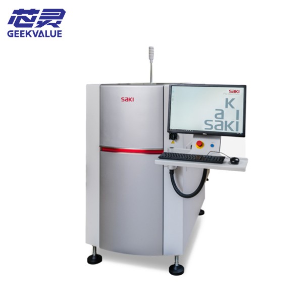
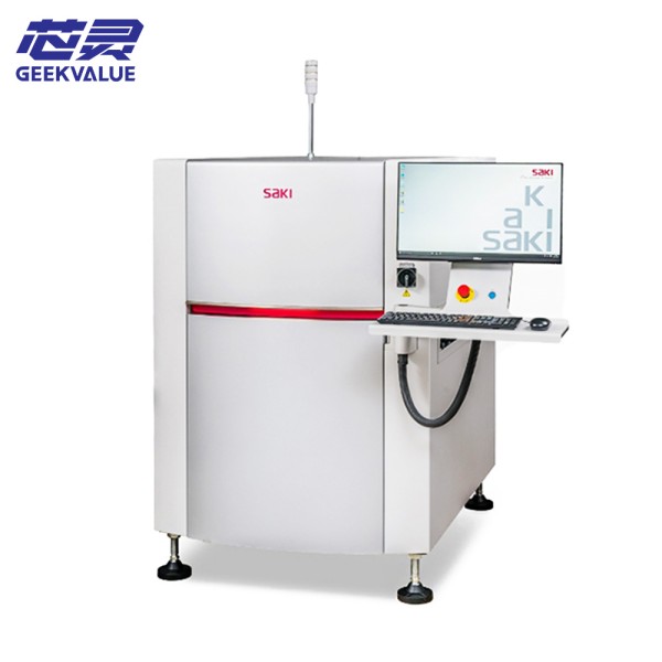
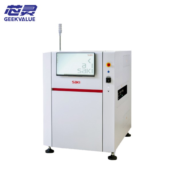
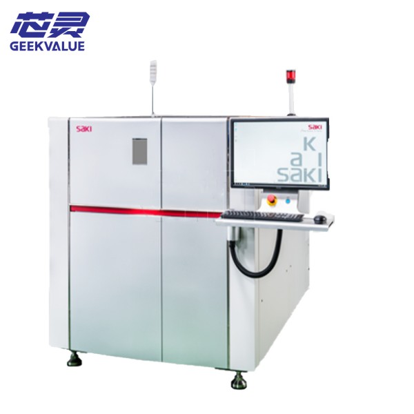
SAKI 3Si-MS2 is a new generation of 3D solder paste inspection system (SPI) launched by SAKI. It adopts innovative multi-spectral measurement technology and is designed for quality control of solder paste printing process in high-precision electro
Why do so many people choose to work with GeekValue?
Our brand is spreading from city to city, and countless people have asked me, "What is GeekValue?" It stems from a simple vision: to empower Chinese innovation with cutting-edge technology. This is a brand spirit of continuous improvement, hidden in our relentless pursuit of detail and the delight of exceeding expectations with every delivery. This almost obsessive craftsmanship and dedication is not only the persistence of our founders, but also the essence and warmth of our brand. We hope you will start here and give us an opportunity to create perfection. Let us work together to create the next "zero defect" miracle.
DetailsAbout Us
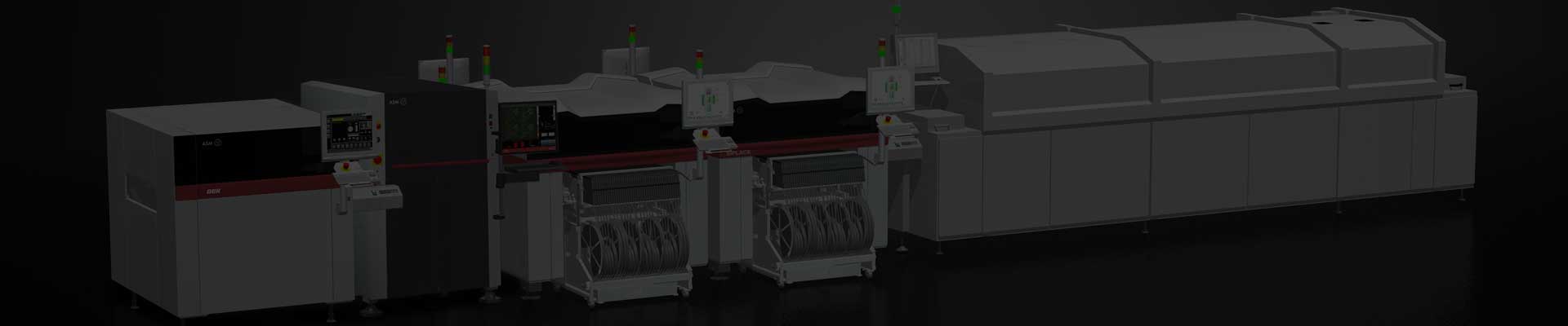
As a supplier of equipment for the electronics manufacturing industry, Geekvalue offers a range of new and used machines and accessories from renowned brands at very competitive prices.
Contact address: No. 18, Shangliao Industrial Road, Shajing Town, Baoan District, Shenzhen, China
Consultation phone number: +86 13823218491
Email: smt-sales3@gdxinling.cn
CONTACT US
© All Rights Reserved. Technical Support:TiaoQingCMS