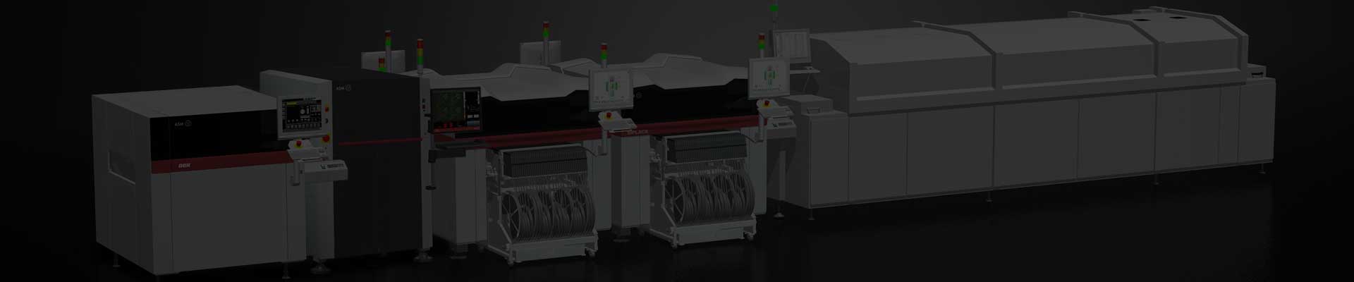
SAKI 3Si-LS2 is an advanced 3D solder paste inspection equipment (SPI) that uses laser triangulation technology and is designed for high-precision solder paste printing process quality control. The equipment can quickly and accurately detect the thickness, area, volume and shape of solder paste before reflow soldering, effectively preventing SMT assembly defects.
2. Core technical specifications
Project parameters
Detection technology: laser triangulation + color imaging
Measurement accuracy: thickness ±1μm, position ±5μm
Scanning speed: up to 800mm/s
Measurement height range: 0-300μm
Minimum detection component: 01005 (0402)
PCB size support: up to 510×460mm
Laser wavelength: 650nm (red laser)
Repeat accuracy: ±0.5μm
Data interface: SECS/GEM, TCP/IP
3. Core advantages
3.1 Ultra-high precision detection
Adopting dual laser scanning system, the thickness measurement accuracy reaches ±1μm
Sub-micron Z-axis resolution, can detect tiny solder paste differences
3.2 Efficient production adaptation
800mm/s high-speed scanning, single board detection time can be controlled within 15 seconds
Intelligent panel recognition, automatic processing of continuous panel detection
3.3 Intelligent data analysis
3D+2D composite analysis, simultaneous thickness and shape parameter evaluation
SPC real-time monitoring, automatic warning of process abnormalities
4. Outstanding features
4.1 Multimodal detection system
Laser scanning: Accurately measure height data
Color imaging: Assist in identifying defects such as solder paste contamination and diffusion
Infrared temperature measurement: Monitor solder paste temperature stability
4.2 Intelligent algorithm
Adaptive threshold: Automatically adjust the detection standard
Virtual measurement: Predict the shape of solder joints after reflow soldering
NG root cause analysis: Automatically trace the cause of defects
4.3 Humanized design
Automatic height alignment system: Adapt to different board thicknesses
Dual-track design: Detection and upper and lower boards are carried out simultaneously
Remote diagnosis: Support manufacturer online technical support
5. Operation precautions
5.1 Environmental requirements
Temperature: 23±3℃
Humidity: 40-60%RH
Cleanliness: Class 10000 and below
Vibration: <0.2G
5.2 Daily operation
Preparation for power on:
Warm up for 15 minutes
Perform automatic calibration
Confirm that the laser power is stable
Test settings:
A standard test library must be established for new models
Regularly verify the effectiveness of the test procedures
Safety regulations:
Do not look directly into the laser beam
Do not open the safety door when the equipment is running
6. Common errors and handling
Error code Fault description Solution
E1101 Laser abnormality 1. Check the laser power supply
2. Contact the manufacturer for maintenance
E1203 Z-axis movement exceeds the limit 1. Check the PCB thickness setting
2. Calibrate the Z-axis sensor
E1305 Communication timeout 1. Check the network cable connection
2. Restart the communication module
E1402 Image acquisition failed 1. Clean the optical window
2. Check the camera connection
E1508 Data storage abnormality 1. Check the hard disk space
2. Restart the system
7. Maintenance method
7.1 Daily maintenance
Daily:
Clean the laser window (use special cleaning paper)
Check the cleanliness of the conveyor track
Confirm the air source pressure (if applicable)
Weekly:
Perform a comprehensive optical calibration
Back up system parameters
Check the cooling fan status
7.2 Regular maintenance
Monthly:
Replace the filter cotton
Lubricate the linear guide
Check the cable connection
Quarterly:
Deeply calibrate the laser system
Replace the aging LED light source
Detect the system ground resistance
7.3 Annual maintenance
Performed by the original engineer:
Laser power calibration
Motion system accuracy detection
Control system firmware upgrade
8. Technical highlights
Dual laser scanning: Eliminate measurement shadows
Real-time 3D modeling: Intuitively display the solder paste status
Intelligent compensation algorithm: Automatically correct the impact of PCB warpage
Process traceability system: Comprehensively record the detection data
9. Application suggestions
High-density board: It is recommended to set the detection resolution to 10μm
Automotive electronics: Use strict detection standards
Flexible board: Use a special carrier to fix
Mass production environment: It is recommended to set the detection resolution to 10μm every 4 Sampling verification is performed once an hour
For detailed operation of this equipment, please refer to the SAKI 3Si-LS2 operation manual. It is recommended that operators complete SAKI certification training. Equipment maintenance requires the use of original factory-specified consumables. Unauthorized modifications may affect detection accuracy
")