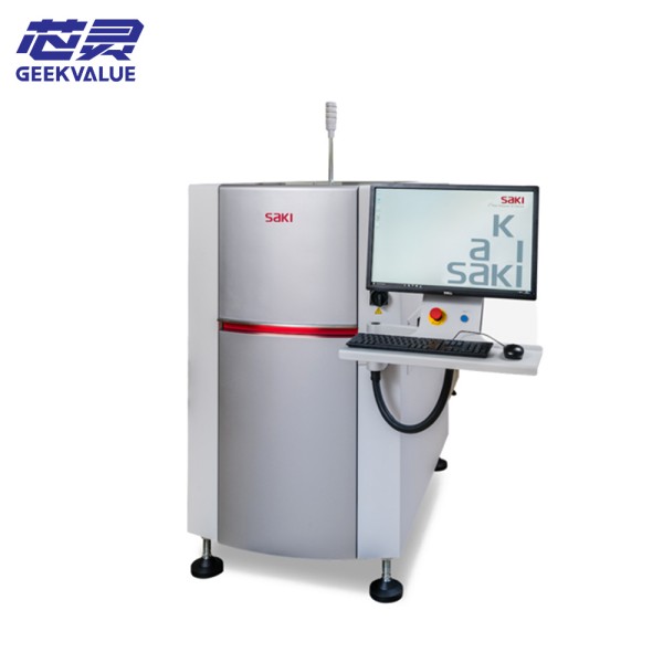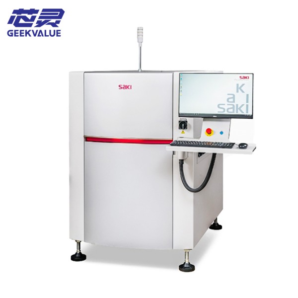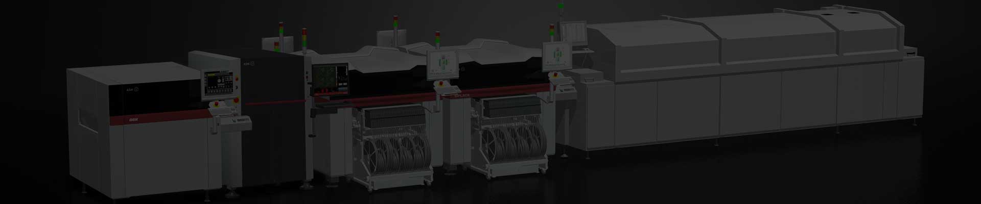
SAKI BF-3Si-L2 is a high-precision 3D solder paste inspection system (SPI) launched by SAKI of Japan, which is specially designed for the quality control of solder paste printing process on SMT production lines. The equipment uses multi-angle 3D imaging technology to accurately measure key parameters such as height, volume, and area of solder paste to ensure that the printing quality meets the requirements of high-density electronic assembly.
Core advantages:
Ultra-high precision: ±1μm height measurement accuracy
High-speed detection: 0.03 seconds/test point (industry leading)
Intelligent closed-loop control: supports automatic parameter adjustment in conjunction with the printer
2. Core specifications and technical parameters
Hardware configuration
Components Specifications Technical features
Optical system Multi-angle laser scanning + high-resolution CCD 3D imaging accuracy ±1μm
Light source Blue laser (405nm) + white light LED Reduce reflection interference
Motion system Linear motor drive Repeat positioning accuracy ±3μm
Detection range Maximum board size 510×460mm Expandable to 610×510mm
Key performance indicators
Parameters Indicators
Minimum detection pad size 0.1×0.1mm
Height measurement range 0-200μm (expandable to 500μm)
Detection speed 0.03 seconds/test point (simple feature)
Measurement accuracy Height ±1μm, volume ±3%
Communication interface SECS/GEM, TCP/IP, PLC I/O
3. System advantages and innovative technologies
Five core advantages
True 3D measurement:
Multi-angle laser triangulation measurement technology is used to eliminate shadow effects
Can detect fine-pitch solder paste (such as 01005 component pads)
AI intelligent analysis:
Automatically identify defects such as solder paste tipping, bridging, and insufficient tin
Support dynamic tolerance adjustment (automatically optimize standards according to pad size)
Closed-loop control:
Real-time data feedback to the printer (supports mainstream brands such as DEK and MPM)
Automatically adjust parameters such as scraper pressure and speed
High speed and high precision:
Patented parallel scanning technology increases detection speed by 30%
0.1μm Z-axis resolution
User-friendly design:
15-inch touch screen operation interface
Support offline programming (does not affect production rhythm)
4. Operation specifications and precautions
Equipment installation requirements
Item Standard requirements
Ambient temperature 20±2℃ (constant temperature workshop)
Humidity range 40-60% RH
Vibration isolation Vibration amplitude <1μm (it is recommended to install anti-vibration pads)
Power supply specifications 220V±5%/50Hz (independent grounding <4Ω)
Daily operation precautions
Power-on process:
First start the host power → preheat for 10 minutes → perform automatic calibration
Use standard height calibration block to verify accuracy every day
PCB placement specifications:
Use vacuum adsorption to fix PCB (to prevent warping from affecting measurement)
Board edge distance to the inner wall of the device ≥30mm
Detection parameter setting:
Select different reflectivity parameters according to solder paste type (SnPb/SAC305)
It is recommended to enable micro-area scanning mode for high-density boards
Safety precautions:
Do not look directly at the laser light source (Class 2M laser protection standard)
Check the emergency stop button function every week
5. Common errors and troubleshooting
Hardware failures
Error code Fault phenomenon Solution
HW101 Laser is not ready Check the laser power connection → Restart the device
HW205 Z-axis movement exceeds the limit Check the PCB thickness setting → Clean the foreign matter on the guide rail
HW308 Camera communication failed Replug the Camera Link cable
Typical detection problem handling
Measurement data fluctuates greatly:
Clean the glass calibration board
Check whether the ambient temperature and humidity are stable
Blurred solder paste edge:
Adjust the laser incident angle (30-45° is recommended)
Update lens focus parameters
6. Typical application cases
Case 1: Smartphone motherboard detection
Challenges:
0.3mm pitch BGA solder paste detection
Require volume control within ±5%
Solution:
Enable micro focus scanning mode (5μm spot diameter)
Set dynamic tolerance band (center area ±3%, edge ±5%)
Case 2: Automobile ECU production
Special requirements:
100% full inspection and data traceability
Detection speed ≤15 seconds/board
Implementation plan:
Use flying scanning technology (continuous detection without stopping)
Direct connection with MES system (automatically generate CPK report)